I've been working on putting together a soldered version of the elevator project I recently completed (to my own satisfaction, that is) using breadboards.
I spent quite a while drawing the circuit, resulting in the following diagram. I used the Fritzing program to draw this. It gives you a blank circuit area to work with, and you can put breadboards into the drawing space and wire your components together.
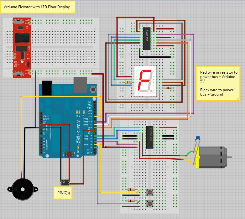
From there, I drew up a circuit diagram on graph paper, and tried to identify the inputs, outputs, and location of the chips. I wanted to have some ribbon cables connecting the Arduino to the circuit board.
Unfortunately, I didn't lay things out very well - I had one of the ribbons going to two different places, and the connectors I bought don't "stick" into the ports on the Arduino - they just fall out. I'll have to do some more investigation into the right kind of connectors before I can continue.
Here are a few pictures of the board - it's super ugly, but these things often are. It's the first one I've done from scratch, so I may be able to improve on it if I go another round with the soldering iron.

Some notes - the circuit diagram and a mock layout on graph paper. The mock layout looked good on paper, as they say, but it didn't work out when I was ready to connect the ribbon cables to the board. Oops!

The beginnings of the board. I have soldered a few components in place, and am in the process of drilling the holes for the buttons.

Same as before, but with the ribbon cables that I want to use to connect the board to the Arduino and power supplies.

The front of the board, with the chips in their sockets and the wires snaking around however I could make them fit. Presumably, there would be a cover over this board so you could only see the buttons and LED display, although on further inspection, most of the other components, and some wires, were almost as tall as those components.

The back of the board, where the ugly happens. The red wire is the positive "bus", and you'll note a few places the insulation was scraped off the wire so I could hook a component directly to it. This, and many other tricks I tried, were found on the internet by other people who can do this and make it look pretty. The black wire, and the associated blobs of solder that form solid lines, is the ground "bus". There are quite a few places in the wiring where components are wired to one or both of the positive/negative buses that I felt it was necessary to run those wires all over the place. The bottoms of the buttons, and some of the chip connections to the buses, were made with leads clipped off of spare components.
I've learned a ton from this experience. My first diagram had the wires on the right side of the LED display one space lower than they should have been, and I had all but the final wire soldered before I realized it. Lots of lessons learned, and my soldering skills are better now, too.
Now - back to researching circuits some more, and then to find some better header connectors to replace the ones I bought. Eventually, I'd like to make one of these:

I don't actually want to make one of these. Just kidding. Dad, recognize this?
---